
INDUSTRIAL X-RAY INSPECTION APPLICATIONS
Start with what needs to be inspected. Explore X-Ray inspection applications for hidden solder joints, semiconductor packages, battery structures and complex industrial components — then connect the inspection requirement to the appropriate SEAMARK technology.
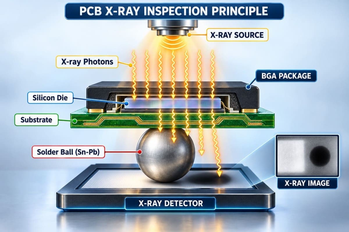
SEE WHAT OPTICAL INSPECTION CANNOT.
Use X-Ray inspection for PCBA / SMT assemblies when solder joints are concealed underneath components such as BGA, QFN and power packages. The objective is to evaluate hidden connections, including voids, bridging, open joints, insufficient solder and misalignment.
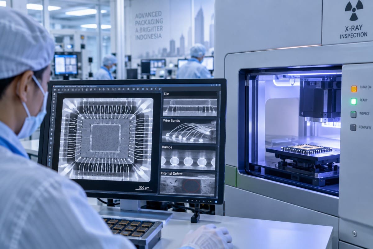
INSPECT BENEATH THE PACKAGE.
X-Ray inspection reveals internal semiconductor structures that external inspection cannot reach. Evaluate die placement, wire bonds, bump arrays, package interconnects and hidden defects across advanced packaging and precision semiconductor manufacturing applications.

SEE INSIDE THE CELL. VERIFY WHAT POWERS THE SYSTEM.
X-Ray inspection supports deeper evaluation of battery cells, weld tabs, electrode alignment, internal structure and module assembly quality. This application path is ideal when manufacturers need better visibility into hidden structures, internal consistency and battery architecture reliability.
INSPECT THE MATERIAL. UNDERSTAND THE DEFECT.
X-Ray inspection provides visibility into castings, welds, precision components, machined parts and mechanical assemblies where internal conditions cannot be judged from the surface alone. Evaluate hidden geometry, porosity, cracks, inclusions, voids and structural integrity before selecting the appropriate inspection architecture.
 POROSITY
CRACK
INTERNAL VOID
WELD INTEGRITY
INTERNAL GEOMETRY
POROSITY
CRACK
INTERNAL VOID
WELD INTEGRITY
INTERNAL GEOMETRY